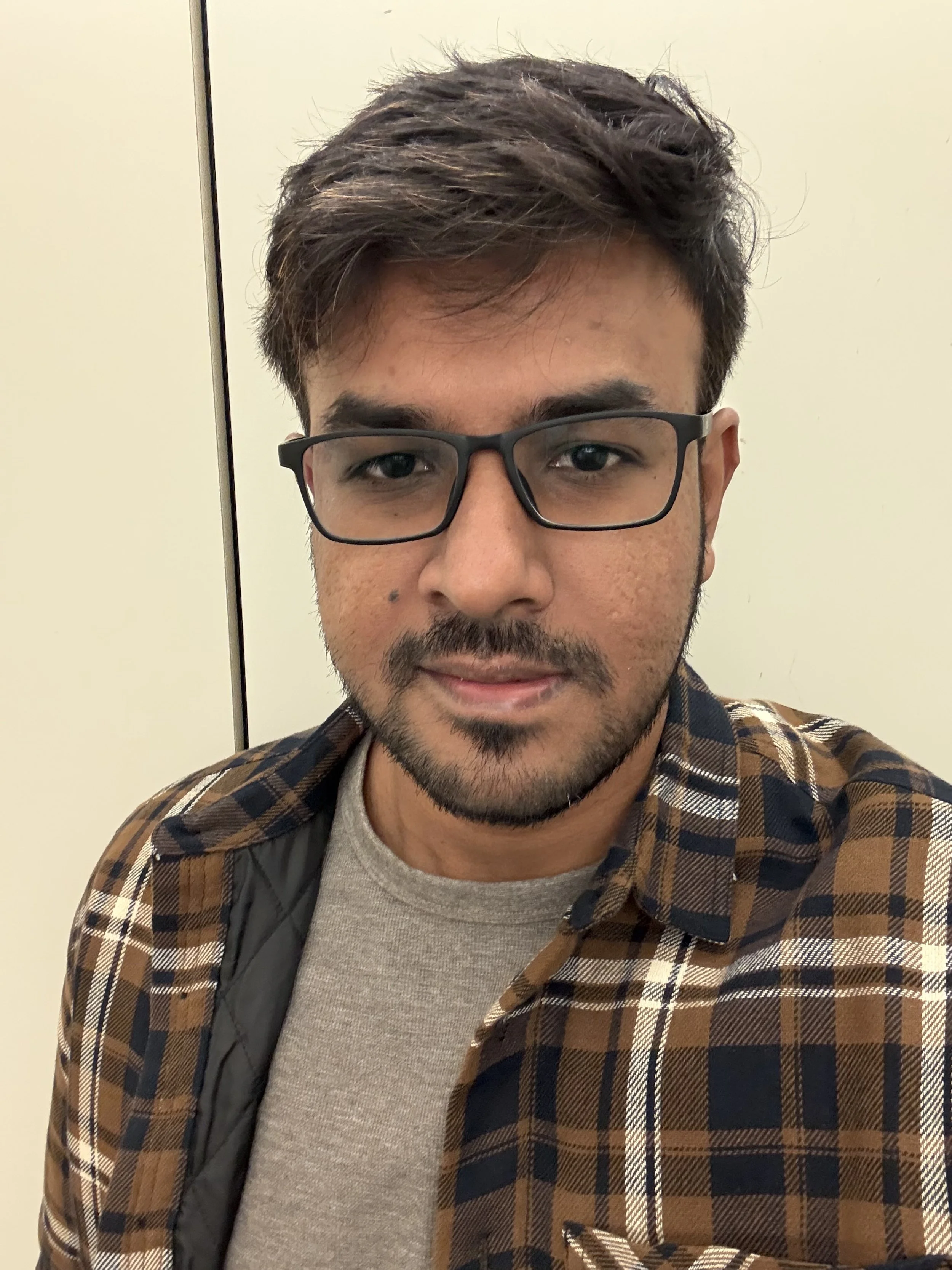
With extensive experience in advanced packaging, heterogeneous integration, and semiconductor process development, I currently serve as a Senior Integration Engineer at the Texas Institute for Electronics, where I lead efforts in toolset qualification, process integration, and yield improvement for next-generation heterogeneous integration prototypes for advancing US leadership in the global semiconductor manufacturing landscape. I am also involved in developing educational programs to train the next generation of skilled workforce in the highly critical field of Advanced Packaging. Previously, I was Deputy Director of UCLA CHIPS, managing daily operations, guiding graduate research, securing funding, and conducting R&D in 3DHI and novel backside power delivery schemes for wafer-scale systems. My background also includes hands-on experimental work in optical packaging and silicon photonics at IIT Madras, as well as patented research on microLED mass transfer for flexible displays at UCLA.
About me:
© Goutham Ezhilarasu
